
Project
Hardware
Manual

MXE11: run UNIX on a microcontroller
V1.71 (c) 2017-2018 Joerg Wolfram
V1.71 (c) 2017-2018 Joerg Wolfram
1 Basic hardware
Hint at the beginning: A 1: 1 replica instruction for all possible variants does not exist, because I usually take the components, which I have got or can 'recycle' from old projects or circuit boards. Only for the STM32F405 variant exists a relatively current layout.
DThe layout is one-sided (with a few jumper wires) and includes the STM32F405RG, an AT45DB642 and an ATMega88 RTC. It is created with gEDA PCB and is located in the doc archive. I have not documented it at the moment, because usually other layout programs are preferred.
1.1 Circuit
The circuit diagram usually only shows the signal designations. As an external disk either an AT45DB642 Dataflash (Binary page mode) or an SD card can be used. The pin assignment on the controller is in both Same cases. TTY8 (/dev/tty8) and TTY0 (/dev/tty0) are currently provided as serial interfaces, whereby TTY8 is the primary console. The connections of the UPROG2 are specified as ISP interface. If an AT45DB642 should be used, I recommend instead of a reset button to set up a detent switch. This can be the used for deactivating the microcontroller during programming of flashes to not interfere with programming.1.2 SPC56EL60
This is the original version that I built with a test board. The quartz frequency is 16MHz, the CPU frequency 120MHz. Currently only 1 core is used.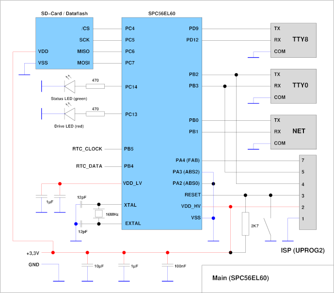
1.3 STM32F103
Trial version on a dedicated SMT32-duino compatible board, crystal frequency is 8MHz. The controller was brought to 120MHz via overclocking, this can be disabled in board.h by commenting #define F1_OVERCLOCKING out.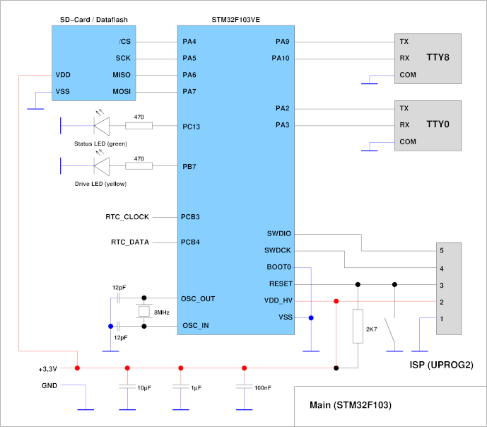
1.4 STM32F107
As a board I used the Olimex STM32-H107 board, quartz frequency is 8MHz. Overclocking did not work stable, therefore 72MHz clock frequency.
1.5 STM32F411
As board I used the STM32F411E Discovery Board, quartz frequency is 8MHz.
1.6 STM32F405
Board here is my designed board for the MXE11, quartz frequency is 16MHz.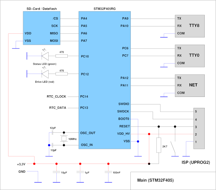
1.7 STM32L475
Board is the same MXE11 board as with the STM32F405, only the signals for TTY0 must be parallel-wired, since they are located on PC4/PC5 instead of PC6/PC7. The crystal frequency is also 16MHz.
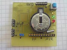
2 The RTC
Although some of the microcontrollers used have an integrated RTC (STM32), I have my own (external) solution that works with all controllers used and planned. Over a 2-wire interface are beside the seconds register (32 bit) 15 additional 32-bit battery-powered registers available for universal use.2.1 Circuit
The center of the circuit is in the current case an ATMega48/88/168/328, the exact type is secondary. The controller runs with internal RC oscillator, in addition, a 32758 Hz watch quartz is necessary. The communication with the host controller takes place via two lines (clock and data), whereby the clock line over an NPN transistor is inverted. The data line contents a decoupling resistor of 1KOhm to avoid signal conflicts during direction switching. The ATMega is powered by a 3V lithium button cell.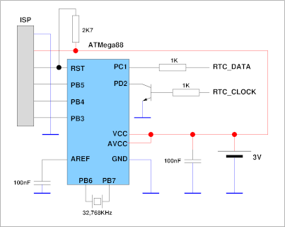
2.2 Protocoll
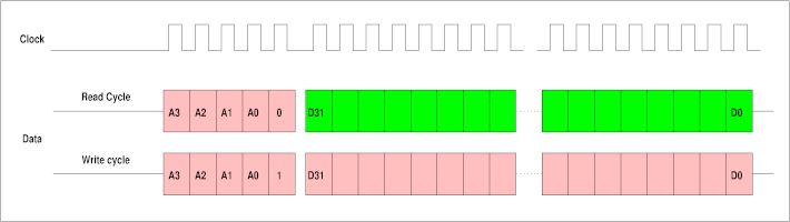
The communication on the part of the host controller takes place via 2 freely selectable I/O pins and on the software side via my Unilib. The RTC controller is in sleep most of the time and is set up at regular intervals woken up via timer 2. Another interrupt source is INT0, which is connected via the external transistor to the Clock line is connected. The maximum clock frequency for the transmission is approx. 16KHz. Since that Reading the RTC only when starting the emulator plays the time required for the communication only a minor role.After this, 4 address bits and one R/W bit are sent clock-synchronously to the RTC. Depending on R/W bit then follow 32 bits of data either from the RTC to the host or from the host to the RTC. Then the communication is completed and the RTC goes back to sleep mode.
In case of incomplete communication, the RTC stopps after approx 0.5 seconds with a timeout and goes back to sleep mode. By this way, short glitches are filtered out.
2.3 Software
The software on the ATMega is written in assembler and uses both Timer 2 and Int0 as wake-up and Interrupt sources.The fuse settings fo an ATMega88 are:
LOW-FUSE 0xD2 HIGH-FUSE 0xDF EXT-FUSE 0xFF |
3 Expansions
As a later extension a network function via CAN, 4 analog inputs, 4 analog outputs (via PWM) and 4 digital inputs / outputs each ar planned. For layouts the corresponding pins should be used already taken into account.It should make sense to realize the I/O as a daughter board, so the layout of the Basic board remains easier. The following tables contain only the intended pins, the concrete circuit theerfor (especially decoupling) is actual not yet defined.
3.1 SPC56EL60
| Signal | Pin |
| CAN TX | PB0 |
| RAN RX | PB1 |
| AIN_0 | PB7 |
| AIN_1 | PB8 |
| AIN_2 | PB9 |
| AIN_3 | PB10 |
| AOUT_0 | PA10 |
| AOUT_1 | PA11 |
| AOUT_2 | PA12 |
| AOUT_3 | PA13 |
| DIN_0 | PB11 |
| DIN_1 | PP12 |
| DIN_2 | PB13 |
| DIN_3 | PB14 |
| DOUT_0 | PA0 |
| DOUT_1 | PA1 |
| DOUT_2 | PD10 |
| DOUT_3 | PD11 |
3.2 STM32F103
This device has no CAN.| Signal | Pin |
| CAN TX | --- |
| RAN RX | --- |
| AIN_0 | PA0 |
| AIN_1 | PA1 |
| AIN_2 | PB0 |
| AIN_3 | PB1 |
| AOUT_0 | PC6 |
| AOUT_1 | PC7 |
| AOUT_2 | PC8 |
| AOUT_3 | PC9 |
| DIN_0 | PC0 |
| DIN_1 | PC1 |
| DIN_2 | PC2 |
| DIN_3 | PC3 |
| DOUT_0 | PB12 |
| DOUT_1 | PB13 |
| DOUT_2 | PB14 |
| DOUT_3 | PB15 |
3.3 STM32F107
I used the Olimex STM32-H107 Board.| Signal | Pin |
| CAN TX | PA12 |
| RAN RX | PA11 |
| AIN_0 | PA0 |
| AIN_1 | PA1 |
| AIN_2 | PB0 |
| AIN_3 | PB1 |
| AOUT_0 | PC6 |
| AOUT_1 | PC7 |
| AOUT_2 | PC8 |
| AOUT_3 | PC9 |
| DIN_0 | PC0 |
| DIN_1 | PC1 |
| DIN_2 | PC2 |
| DIN_3 | PC3 |
| DOUT_0 | PB12 |
| DOUT_1 | PB13 |
| DOUT_2 | PB14 |
| DOUT_3 | PB15 |
3.4 STM32F411
I used the STM32F411E-Discovery Board, at this time (v1.71) the signals are not defined.3.5 STM32F405
This device will get its own board (planned).| Signal | Pin |
| CAN TX | PA12 |
| RAN RX | PA11 |
| AIN_0 | PC4 |
| AIN_1 | PC5 |
| AIN_2 | PB0 |
| AIN_3 | PB1 |
| AOUT_0 | PC6 |
| AOUT_1 | PC7 |
| AOUT_2 | PC8 |
| AOUT_3 | PC9 |
| DIN_0 | PC0 |
| DIN_1 | PC1 |
| DIN_2 | PC2 |
| DIN_3 | PC3 |
| DOUT_0 | PB12 |
| DOUT_1 | PB13 |
| DOUT_2 | PB14 |
| DOUT_3 | PB15 |
3.6 STM32L475
No board and no pin specified.created with latex2web.pl v0.63 © 2006-2018 Joerg Wolfram